

India Is Becoming a Semiconductor Hub.
Vidwath School of AI is pioneering semiconductor systems and preparing engineering talent for India's growing semiconductor ecosystem, from chip design to manufacturing.
Semiconductor Training, Internship & Placement Program
Explore a structured learning pathway designed to connect engineering education with the evolving semiconductor industry.
- Build Your Future in Semiconductor Engineering.
A six-month, fully offline Semiconductor & VLSI Internship and Placement Program in Mysuru, offering hands-on training, lab access, real-world project experience and exposure to industry-standard EDA tools.
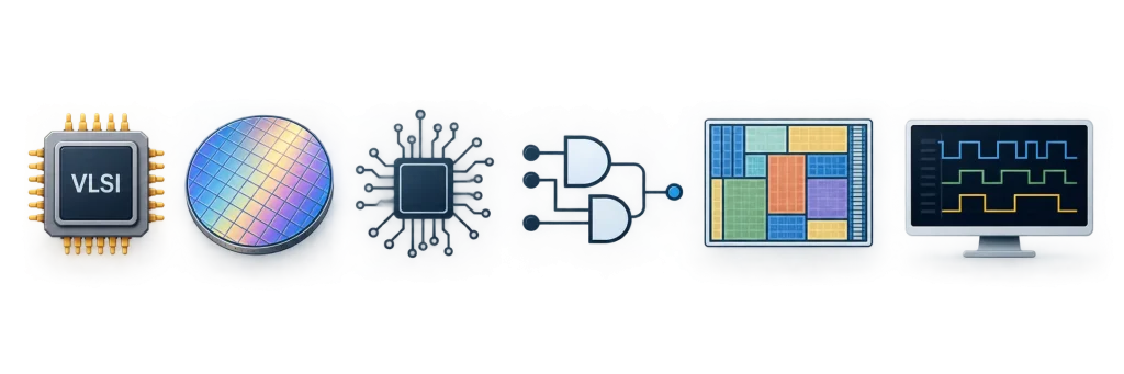
- Practical Learning
- Industry Engagement
- Research & Innovation
- Career Development
What You'll Learn & Build
Progress from digital design fundamentals to physical implementation, then apply your skills through an eight-week guided VLSI project.
Digital & CMOS Foundations
Build a strong foundation in digital logic, combinational and sequential circuits, CMOS fundamentals, standard cells and introductory Verilog.
Skills Covered: Digital Logic, Boolean Design, CMOS Fundamentals, Verilog, Linux, Git
RTL Design & Verification
Develop synthesizable RTL, understand hardware architecture, build self-checking testbenches and explore assertions, coverage and clock-domain crossing.
Skills Covered: RTL Design, SystemVerilog, FSMs, Testbenches, Assertions, CDC
Synthesis, STA, DFT & Low Power
Translate RTL into a technology-mapped design, define timing constraints, analyse setup and hold paths, and understand design-for-test and low-power techniques.
Skills Covered: Logic Synthesis, SDC Constraints, Static Timing Analysis, DFT, Power Analysis
Physical Design & Signoff
Take a synthesized design through floorplanning, power planning, placement, clock-tree synthesis, routing, extraction and physical verification.
Skills Covered: Floorplanning, Placement, CTS, Routing, DRC/LVS, PPA Analysis
Capstone Project: Design & Verification
Begin a mentored semiconductor design project. Define specifications, plan the architecture, develop RTL and build a verification environment with measurable results.
Project Focus: Architecture, RTL Implementation, Verification Closure, Assertions, Coverage
Project Signoff & Placement Preparation
Complete your capstone project through physical implementation and signoff, document your results, and prepare for semiconductor career opportunities with focused interview preparation and placement support.
Focus Areas: Physical Design, PPA Analysis, Project Presentation, Resume Preparation, Technical Interviews, Placement Support
Build practical VLSI design skills through structured training, guided laboratory work and an end-to-end capstone project.
Is Semiconductor Engineering Right for You?
Whether you’re an engineering graduate, a final-year student or a working professional, explore your pathway into semiconductor engineering through specialised training and practical learning.
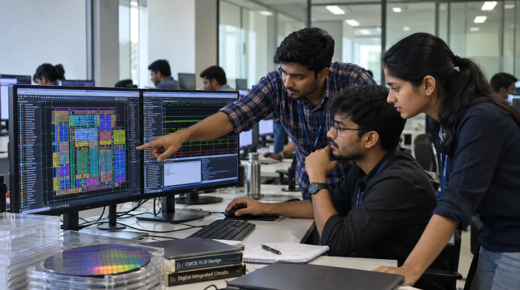
Engineering Graduates
B.E. or B.Tech graduates in ECE, EEE and related electronics engineering disciplines looking to specialise in semiconductor design.
Final Year Students
Students preparing to build core technical skills and explore entry-level opportunities in semiconductor and VLSI engineering.
Working Professionals
Professionals looking to strengthen their semiconductor knowledge, build specialised skills or explore a career transition.
Open to All Passionate Learners. We value your willingness to learn and commitment to building a career in semiconductor engineering.
Your Learning Journey in Semiconductor and VLSI Engineering
Explore RTL design, verification, synthesis and physical design through hands-on projects using Industry-Standard EDA Tools.
Building India's Semiconductor Ecosystem
Build practical semiconductor and VLSI skills through hands-on training, dedicated lab access and industry-relevant design workflows across Vidwath’s expanding learning centres.
Dedicated Semiconductor Labs
Hands-on semiconductor training in dedicated, well-equipped lab environments.
End-to-End VLSI Training
Learn RTL design, verification, synthesis, physical design and GDSII tape-out.
Industry-Standard EDA Tools
Gain practical experience with professional semiconductor design tools.
Projects & Career Support
Build project experience with internship and placement support.

Everything You Need to Know About the Program
Find answers about our Semiconductor and VLSI training, curriculum, practical learning, internship and career support.

A six-month, full-time offline program focused on semiconductor design, VLSI workflows, hands-on projects, internship experience and placement support.
Engineering students and graduates interested in semiconductor and VLSI careers, particularly those from ECE, EEE and related engineering disciplines.
The program runs for six months and follows a full-time, offline training format.
The curriculum covers semiconductor fundamentals, RTL design, design verification, synthesis, static timing analysis, physical design and GDSII tape-out concepts.
Yes. The program includes practical exposure to industry-standard EDA tools through guided exercises, lab sessions and project work.
Yes. The program includes an internship component and practical project experience.
Yes. Our program focuses on preparing participants for semiconductor and VLSI careers through industry-oriented training, hands-on project experience, internship opportunities, interview preparation, and dedicated placement support.
Ready to Begin Your Journey in Semiconductor Engineering?
Explore six months of offline Semiconductor and VLSI training, practical project work and industry EDA tool exposure at Vidwath’s Mysuru Centre of Excellence.
- 6-month program
- Practical Learning
- Career Pathways